A compact antenna front end is a great Zener example because it uses all three
layers of the language:
- thin
Component() wrappers for custom physical parts
- a reusable
Module() for the matching network
- a top-level
Board() that composes the RF path
This guide follows the board repository and package model from the
language spec. In particular:
- the top-level design uses
Board(...), not Layout(...)
- reusable blocks live in packages under
modules/ and components/
- local imports use normal paths
Repository Layout
Start with a normal board repository and give each reusable block its own package:
my-rf-demo/
├── pcb.toml
├── AntennaDemo.zen
├── modules/
│   └── AntennaMatch/
│       ├── AntennaMatch.zen
│       └── pcb.toml
└── components/
    ├── ChipAntenna/
    │   ├── ChipAntenna.zen
    │   └── pcb.toml
    └── SMAConnector/
        ├── SMAConnector.zen
        └── pcb.toml
pcb.toml can be as small as:
[workspace]
pcb-version = "0.3"

[board]
name = "AntennaDemo"
path = "AntennaDemo.zen"
description = "Replace with concise board description."
Use pcb new board and pcb new package to create this structure. The values
in this guide are starting points only. Real matching values should come from
your antenna datasheet, PCB stackup, and VNA measurements.
1. Wrap The Physical Endpoints
For common passives, prefer the stdlib generics. For parts like an SMA connector
or a specific chip antenna, a tiny custom package is often the right tool.
Each .zen file is still a module. A custom “component package” is simply a
small module that calls Component() once and exposes its pins through io().
SMA Connector
# components/SMAConnector/SMAConnector.zen
CENTER = io(Net, help="Coax center conductor")
SHIELD = io(Ground, help="Coax shield")

prefix = config(str, default="J")

Component(
    name = "SMAConnector",
    symbol = Symbol(
        library = "@kicad-symbols/Connector.kicad_sym",
        name = "Conn_Coaxial_Small",
    ),
    footprint = File(
        "@kicad-footprints/Connector_Coaxial.pretty/SMA_Amphenol_132134_Vertical.kicad_mod"
    ),
    prefix = prefix,
    pins = {
        "In": CENTER,
        "Ext": SHIELD,
    },
)
Chip Antenna
# components/ChipAntenna/ChipAntenna.zen
FEED = io(Net)

prefix = config(str, default="AE")

Component(
    name = "ChipAntenna",
    symbol = Symbol(
        library = "@kicad-symbols/Device.kicad_sym",
        name = "Antenna",
    ),
    footprint = File(
        "@kicad-footprints/RF_Antenna.pretty/Texas_SWRA416_868MHz_915MHz.kicad_mod"
    ),
    prefix = prefix,
    pins = {
        "A": FEED,
    },
)
Use raw Component() only for the parts that actually need it. The matching
elements themselves should stay on the stdlib generics so you inherit current
symbols, footprints, and BOM behavior automatically.
If you are authoring these files in the editor, hovering the pins field in a
Component() call will show the pin names Zener expects from the symbol.
2. Build A Reusable Matching Module
This matching block reserves three tuning footprints: a series inductor, a
shunt capacitor, and a final series resistor that can be used as a real damping
element or simply stuffed as 0ohm.
# modules/AntennaMatch/AntennaMatch.zen
load("@stdlib/units.zen", "Capacitance", "Inductance", "Resistance")

Capacitor = Module("@stdlib/generics/Capacitor.zen")
Inductor = Module("@stdlib/generics/Inductor.zen")
Resistor = Module("@stdlib/generics/Resistor.zen")

series_l = config(Inductance, default=Inductance("6.8nH"))
shunt_c = config(Capacitance, default=Capacitance("1.5pF"))
series_r = config(Resistance, default=Resistance("0ohm"))
package = config(str, default="0402")

RF_IN = io(Net, direction="input")
RF_OUT = io(Net, direction="output")
GND = io(Ground)
MATCH_NODE = Net()

Inductor(
    name = "L_SERIES",
    value = series_l,
    package = package,
    P1 = RF_IN,
    P2 = MATCH_NODE,
)

Capacitor(
    name = "C_SHUNT",
    value = shunt_c,
    package = package,
    P1 = MATCH_NODE,
    P2 = GND,
)

Resistor(
    name = "R_SERIES",
    value = series_r,
    package = package,
    P1 = MATCH_NODE,
    P2 = RF_OUT,
)

Layout(name = "AntennaMatch", path = "layout/AntennaMatch")
Use io() for the nets the parent board must connect, and plain Net() for
internal nodes like MATCH_NODE that should stay inside the module boundary.
The parent can still pass strings like "6.8nH", "1.5pF", and "0ohm".
Zener will convert them to physical quantities because the config() types are
declared explicitly.
3. Compose The Board
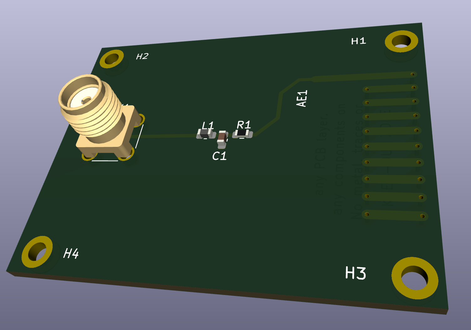
Now instantiate the connector, matching network, and antenna on a real board:
# AntennaDemo.zen
SMAConnector = Module("./components/SMAConnector/SMAConnector.zen")
ChipAntenna = Module("./components/ChipAntenna/ChipAntenna.zen")
AntennaMatch = Module("./modules/AntennaMatch/AntennaMatch.zen")

rf_source = Net("RF_SOURCE")
rf_feed = Net("RF_FEED")
gnd = Ground("GND")

SMAConnector(
    name = "J_RF",
    CENTER = rf_source,
    SHIELD = gnd,
)

AntennaMatch(
    name = "MATCH",
    RF_IN = rf_source,
    RF_OUT = rf_feed,
    GND = gnd,
    series_l = "6.8nH",
    shunt_c = "1.5pF",
    series_r = "0ohm",
    package = "0402",
    schematic = "embed",
)

ChipAntenna(
    name = "AE1",
    FEED = rf_feed,
)

Board(
    name = "AntennaDemo",
    layers = 2,
    layout_path = "layout/AntennaDemo",
)
SMA center -> series inductor -> tuning node -> series resistor -> antenna feed
                                 |
                            shunt capacitor
                                 |
                               ground
Build And Iterate
Build and lay out the board with the normal CLI flow:
pcb build AntennaDemo.zen
pcb layout AntennaDemo.zen
Electrical correctness here depends heavily on placement. In practice, keep the
matching parts as close to the antenna feed as possible, route the RF trace with
the impedance your stackup expects, and leave room for value swaps during bringup.
Bonus: Add Mounting Holes
You can also add mounting holes programmatically:
MountingHole = Module("@stdlib/generics/MountingHole.zen")

for i in range(4):
    MountingHole(
        name = "H" + str(i + 1),
        diameter = "M2",
    )
pcb layout again and place the generated holes where they make sense for
your enclosure and keep-out requirements.
Why This Pattern Scales
- The antenna and connector packages stay small and easy to reuse.
- The matching network owns the topology and tuning values.
- The board file stays focused on composition instead of implementation detail.
That separation is the main benefit of Zener for RF work: you can change
matching values, footprints, or even the whole antenna package without rewriting
the board-level connectivity.