> ## Documentation Index
> Fetch the complete documentation index at: https://docs.pcb.new/llms.txt
> Use this file to discover all available pages before exploring further.
# Antenna matching network
> Build a reusable RF matching network with modern Zener packages
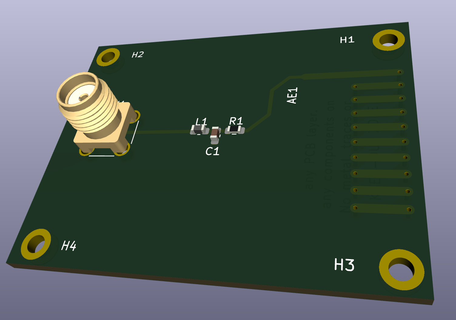
This guide builds an antenna signal path from three Zener elements:
* `Component()` wrappers for the connector and antenna
* a reusable matching-network module
* a board that connects the complete RF path
The example uses the repository model defined in the
[language specification](/pages/spec): the board calls `Board()`, reusable
blocks live under `modules/` and `components/`, and local modules use relative
paths.
 ## Repository layout
Create one package for each reusable block:
```text theme={null}
my-rf-demo/
├── pcb.toml
├── AntennaDemo.zen
├── modules/
│ └── AntennaMatch/
│ ├── AntennaMatch.zen
│ └── pcb.toml
└── components/
├── ChipAntenna/
│ ├── ChipAntenna.zen
│ ├── ChipAntenna.kicad_sym
│ ├── ChipAntenna.kicad_mod
│ └── pcb.toml
└── SMAConnector/
├── SMAConnector.zen
├── SMAConnector.kicad_sym
├── SMAConnector.kicad_mod
└── pcb.toml
```
The root `pcb.toml` can be as small as:
```toml theme={null}
[workspace]
pcb-version = "0.4"
[board]
name = "AntennaDemo"
path = "AntennaDemo.zen"
description = "Replace with concise board description."
```
Use `pcb new board` and `pcb new package` to create this structure. The component
values below are examples. Select production values from the antenna data,
finished PCB stackup, and vector network analyzer measurements.
Before writing Zener source, copy the KiCad symbol and footprint for each
physical part into its package directory with the filenames shown above. Zener
does not copy these assets from an installed KiCad library. Confirm that the
symbol pin names match the wrapper's `pins` mapping.
## 1. Wrap the physical endpoints
Use standard-library generics for common passives. Use a small custom module for
the specific SMA connector and antenna. Each wrapper calls `Component()` once
and exposes the required pins through `io()`.
### SMA connector
```python theme={null}
# components/SMAConnector/SMAConnector.zen
CENTER = io(Net, help="Coax center conductor")
SHIELD = io(Ground, help="Coax shield")
prefix = config(str, default="J")
Component(
name = "SMAConnector",
symbol = Symbol(
library = "SMAConnector.kicad_sym",
),
footprint = File("SMAConnector.kicad_mod"),
prefix = prefix,
pins = {
"In": CENTER,
"Ext": SHIELD,
},
)
```
### Chip antenna
```python theme={null}
# components/ChipAntenna/ChipAntenna.zen
FEED = io(Net)
prefix = config(str, default="AE")
Component(
name = "ChipAntenna",
symbol = Symbol(
library = "ChipAntenna.kicad_sym",
),
footprint = File("ChipAntenna.kicad_mod"),
prefix = prefix,
pins = {
"A": FEED,
},
)
```
Use raw `Component()` only when a standard-library generic does not represent
the physical part. Standard-library generics provide maintained symbols,
footprints, and BOM behavior for the matching components.
Hover over `pins` in the editor to inspect the pin names loaded from the symbol.
## 2. Build the matching module
The module reserves three tuning footprints: a series inductor, a shunt
capacitor, and a final series resistor. Populate the resistor with a damping
value or with `0ohm`.
```python theme={null}
# modules/AntennaMatch/AntennaMatch.zen
load("@stdlib/units.zen", "Capacitance", "Inductance", "Resistance")
Capacitor = Module("@stdlib/generics/Capacitor.zen")
Inductor = Module("@stdlib/generics/Inductor.zen")
Resistor = Module("@stdlib/generics/Resistor.zen")
series_l = config(Inductance, default=Inductance("6.8nH"))
shunt_c = config(Capacitance, default=Capacitance("1.5pF"))
series_r = config(Resistance, default=Resistance("0ohm"))
package = config(str, default="0402")
RF_IN = io(Net, direction="input")
RF_OUT = io(Net, direction="output")
GND = io(Ground)
MATCH_NODE = Net()
Inductor(
name = "L_SERIES",
value = series_l,
package = package,
P1 = RF_IN,
P2 = MATCH_NODE,
)
Capacitor(
name = "C_SHUNT",
value = shunt_c,
package = package,
P1 = MATCH_NODE,
P2 = GND,
)
Resistor(
name = "R_SERIES",
value = series_r,
package = package,
P1 = MATCH_NODE,
P2 = RF_OUT,
)
Layout(name = "AntennaMatch", path = "layout/AntennaMatch")
```
Use `io()` for parent connections and `Net()` for internal nodes such as
`MATCH_NODE`.
The declared `config()` types convert parent-supplied strings such as `"6.8nH"`,
`"1.5pF"`, and `"0ohm"` to physical quantities.
## 3. Compose the board
Instantiate the connector, matching network, and antenna in the board file:
```python theme={null}
# AntennaDemo.zen
SMAConnector = Module("./components/SMAConnector/SMAConnector.zen")
ChipAntenna = Module("./components/ChipAntenna/ChipAntenna.zen")
AntennaMatch = Module("./modules/AntennaMatch/AntennaMatch.zen")
rf_source = Net("RF_SOURCE")
rf_feed = Net("RF_FEED")
gnd = Ground("GND")
SMAConnector(
name = "J_RF",
CENTER = rf_source,
SHIELD = gnd,
)
AntennaMatch(
name = "MATCH",
RF_IN = rf_source,
RF_OUT = rf_feed,
GND = gnd,
series_l = "6.8nH",
shunt_c = "1.5pF",
series_r = "0ohm",
package = "0402",
schematic = "embed",
)
ChipAntenna(
name = "AE1",
FEED = rf_feed,
)
Board(
name = "AntennaDemo",
layers = 2,
layout_path = "layout/AntennaDemo",
)
```
The resulting RF path is:
```text theme={null}
SMA center -> series inductor -> tuning node -> series resistor -> antenna feed
|
shunt capacitor
|
ground
```
## 4. Build and lay out the board
Run these commands from the repository root:
```bash theme={null}
pcb build AntennaDemo.zen
pcb layout AntennaDemo.zen
```
`pcb build` validates the design. `pcb layout` generates the KiCad board and
opens it for placement and routing.
RF performance depends on placement and stackup. Place the matching components
close to the antenna feed, route the RF trace for the required impedance, and
leave access for component changes during bringup.
## Optional mounting holes
Add mounting holes with the standard-library generic:
```python theme={null}
MountingHole = Module("@stdlib/generics/MountingHole.zen")
for i in range(4):
MountingHole(
name = "H" + str(i + 1),
diameter = "M2",
)
```
Run `pcb layout` again, then place the holes to satisfy the enclosure and copper
keep-out requirements.
## Design rationale
* The antenna and connector packages contain only physical-part definitions.
* The matching network owns the topology and tuning values.
* The board file contains only board-level composition.
This separation permits changes to matching values, footprints, or the antenna
package without changing board-level connectivity.
## Repository layout
Create one package for each reusable block:
```text theme={null}
my-rf-demo/
├── pcb.toml
├── AntennaDemo.zen
├── modules/
│ └── AntennaMatch/
│ ├── AntennaMatch.zen
│ └── pcb.toml
└── components/
├── ChipAntenna/
│ ├── ChipAntenna.zen
│ ├── ChipAntenna.kicad_sym
│ ├── ChipAntenna.kicad_mod
│ └── pcb.toml
└── SMAConnector/
├── SMAConnector.zen
├── SMAConnector.kicad_sym
├── SMAConnector.kicad_mod
└── pcb.toml
```
The root `pcb.toml` can be as small as:
```toml theme={null}
[workspace]
pcb-version = "0.4"
[board]
name = "AntennaDemo"
path = "AntennaDemo.zen"
description = "Replace with concise board description."
```
Use `pcb new board` and `pcb new package` to create this structure. The component
values below are examples. Select production values from the antenna data,
finished PCB stackup, and vector network analyzer measurements.
Before writing Zener source, copy the KiCad symbol and footprint for each
physical part into its package directory with the filenames shown above. Zener
does not copy these assets from an installed KiCad library. Confirm that the
symbol pin names match the wrapper's `pins` mapping.
## 1. Wrap the physical endpoints
Use standard-library generics for common passives. Use a small custom module for
the specific SMA connector and antenna. Each wrapper calls `Component()` once
and exposes the required pins through `io()`.
### SMA connector
```python theme={null}
# components/SMAConnector/SMAConnector.zen
CENTER = io(Net, help="Coax center conductor")
SHIELD = io(Ground, help="Coax shield")
prefix = config(str, default="J")
Component(
name = "SMAConnector",
symbol = Symbol(
library = "SMAConnector.kicad_sym",
),
footprint = File("SMAConnector.kicad_mod"),
prefix = prefix,
pins = {
"In": CENTER,
"Ext": SHIELD,
},
)
```
### Chip antenna
```python theme={null}
# components/ChipAntenna/ChipAntenna.zen
FEED = io(Net)
prefix = config(str, default="AE")
Component(
name = "ChipAntenna",
symbol = Symbol(
library = "ChipAntenna.kicad_sym",
),
footprint = File("ChipAntenna.kicad_mod"),
prefix = prefix,
pins = {
"A": FEED,
},
)
```
Use raw `Component()` only when a standard-library generic does not represent
the physical part. Standard-library generics provide maintained symbols,
footprints, and BOM behavior for the matching components.
Hover over `pins` in the editor to inspect the pin names loaded from the symbol.
## 2. Build the matching module
The module reserves three tuning footprints: a series inductor, a shunt
capacitor, and a final series resistor. Populate the resistor with a damping
value or with `0ohm`.
```python theme={null}
# modules/AntennaMatch/AntennaMatch.zen
load("@stdlib/units.zen", "Capacitance", "Inductance", "Resistance")
Capacitor = Module("@stdlib/generics/Capacitor.zen")
Inductor = Module("@stdlib/generics/Inductor.zen")
Resistor = Module("@stdlib/generics/Resistor.zen")
series_l = config(Inductance, default=Inductance("6.8nH"))
shunt_c = config(Capacitance, default=Capacitance("1.5pF"))
series_r = config(Resistance, default=Resistance("0ohm"))
package = config(str, default="0402")
RF_IN = io(Net, direction="input")
RF_OUT = io(Net, direction="output")
GND = io(Ground)
MATCH_NODE = Net()
Inductor(
name = "L_SERIES",
value = series_l,
package = package,
P1 = RF_IN,
P2 = MATCH_NODE,
)
Capacitor(
name = "C_SHUNT",
value = shunt_c,
package = package,
P1 = MATCH_NODE,
P2 = GND,
)
Resistor(
name = "R_SERIES",
value = series_r,
package = package,
P1 = MATCH_NODE,
P2 = RF_OUT,
)
Layout(name = "AntennaMatch", path = "layout/AntennaMatch")
```
Use `io()` for parent connections and `Net()` for internal nodes such as
`MATCH_NODE`.
The declared `config()` types convert parent-supplied strings such as `"6.8nH"`,
`"1.5pF"`, and `"0ohm"` to physical quantities.
## 3. Compose the board
Instantiate the connector, matching network, and antenna in the board file:
```python theme={null}
# AntennaDemo.zen
SMAConnector = Module("./components/SMAConnector/SMAConnector.zen")
ChipAntenna = Module("./components/ChipAntenna/ChipAntenna.zen")
AntennaMatch = Module("./modules/AntennaMatch/AntennaMatch.zen")
rf_source = Net("RF_SOURCE")
rf_feed = Net("RF_FEED")
gnd = Ground("GND")
SMAConnector(
name = "J_RF",
CENTER = rf_source,
SHIELD = gnd,
)
AntennaMatch(
name = "MATCH",
RF_IN = rf_source,
RF_OUT = rf_feed,
GND = gnd,
series_l = "6.8nH",
shunt_c = "1.5pF",
series_r = "0ohm",
package = "0402",
schematic = "embed",
)
ChipAntenna(
name = "AE1",
FEED = rf_feed,
)
Board(
name = "AntennaDemo",
layers = 2,
layout_path = "layout/AntennaDemo",
)
```
The resulting RF path is:
```text theme={null}
SMA center -> series inductor -> tuning node -> series resistor -> antenna feed
|
shunt capacitor
|
ground
```
## 4. Build and lay out the board
Run these commands from the repository root:
```bash theme={null}
pcb build AntennaDemo.zen
pcb layout AntennaDemo.zen
```
`pcb build` validates the design. `pcb layout` generates the KiCad board and
opens it for placement and routing.
RF performance depends on placement and stackup. Place the matching components
close to the antenna feed, route the RF trace for the required impedance, and
leave access for component changes during bringup.
## Optional mounting holes
Add mounting holes with the standard-library generic:
```python theme={null}
MountingHole = Module("@stdlib/generics/MountingHole.zen")
for i in range(4):
MountingHole(
name = "H" + str(i + 1),
diameter = "M2",
)
```
Run `pcb layout` again, then place the holes to satisfy the enclosure and copper
keep-out requirements.
## Design rationale
* The antenna and connector packages contain only physical-part definitions.
* The matching network owns the topology and tuning values.
* The board file contains only board-level composition.
This separation permits changes to matching values, footprints, or the antenna
package without changing board-level connectivity.